The operating principle of series resonant circuit design? Wuhan UHV specializes in the production of series resonance, with a wide range of product selection and professional electrical testing. To find series resonance, choose Wuhan UHV.
Series resonance and parallel resonance are widely used in the design of induction heating power supplies. These two design schemes each have their own advantages and characteristics. The following mainly analyzes the operating status, characteristics, and advantages of the series resonant induction heating power inverter.
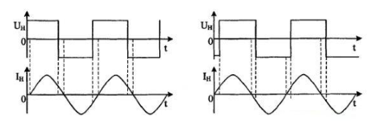
In a series resonant induction heating power supply, the output voltage of the inverter of the body is approximately a square wave during the display process. As the circuit operates near the resonant frequency, the oscillation circuit has the minimum impedance to the fundamental wave, so the load current j is approximately a sine wave. At the same time, to avoid direct connection between the upper and lower bridge arms of the inverter, the commutation must follow the principle of first turning off and then turning on, and there must be sufficient dead time between turning off and turning on.

(a) Inductive load (b) Capacitive load
The above figure shows the output waveforms of capacitive load and inductive load respectively. From the above figure, we can see that when the induction heating power inverter with a series resonant structure operates under a capacitive load, its waveform is shown in Figure (b). It can be seen from the figure that when it operates under a capacitive load state, the phase of the output current leads the voltage phase. Therefore, when the load voltage is still positive, the current crosses zero first, and the commutation between the upper and lower bridge arms changes from the diode of the upper (lower) bridge arm to the MOSFE of the lower (upper) bridge arm.
Due to the slow reverse recovery characteristics of MOSFE parasitic anti parallel diodes, a large reverse recovery current is generated during commutation, resulting in significant switching losses of the device. Moreover, when the reverse recovery current of the diode rapidly drops to zero, a large induced potential is generated in the parasitic inductance connected in series with the MOSFET, causing the MOSFET to be subjected to high voltage spikes.


